It's crystal clear
-
- from Shaastra :: vol 03 issue 10 :: Nov 2024

New mechanism of transforming materials from crystal to amorphous could revolutionise data storage.
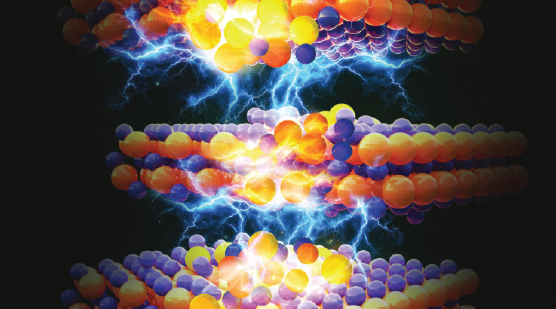
In a development that may revolutionise non-volatile memory technology, a team of researchers has shown that passing small amounts of electric current can transform two-dimensional (2D) indium selenide nanowires from crystalline to glassy (amorphous) form.
The work, reported in Nature in November (bit.ly/nukala), may lead to more sustainable means of data storage. Such transformation from a crystalline to an amorphous form lies at the heart of memory devices such as computer RAMs. Conventionally, a melt-quench process is used to convert crystal to glass and this requires nearly a billion times more power than the method developed by Pavan Nukala, Assistant Professor at the Indian Institute of Science (IISc) in Bengaluru, Ritesh Agarwal, Professor at the University of Pennsylvania in the U.S., and team. They discovered that when an electric current is passed through wires made of indium selenide, a 2D ferroelectric material, long stretches of the material suddenly amorphise into glass.
Indium selenide belongs to a class of materials called chalcogenides (chemical compounds containing at least one element from Group 6 of the Periodic Table such as sulphur, selenium and tellurium and an electropositive element such as germanium and indium), known for their remarkable electronic, optical and semiconducting properties. As they can switch between crystalline and amorphous forms, they are ideal for phase-change memory, a technology that could transform data storage in devices from cell phones to computers.
Self-shock assisted glass formation is a billion times more power-efficient than the conventional way.
"The material should be 2D in nature, meaning that there is a weak van der Waals bonding between some layers of the material, and it should be piezoelectric as well as ferroelectric," Nukala says. Indium selenide is a semiconductor with all these unusual properties. It is 2D, ferroelectric (it can spontaneously polarise and these polarisations can rotate easily with field) and piezoelectric (any electric charge deforms the material).
"When you apply current, the layers will start sliding against each other. This will create defects, which when in large density will lead to a collapse of the (crystalline) structure locally. The intersection of certain defects, also self-shocks the material (analogous to creation of an earthquake when tectonic plates slide against each other)," Nukala says. "These shocks propagate disorder in a much longer range, replicating the local pockets of amorphisation to occur in a lot more regions of the material. At some point they start percolating, turning the entire 2D material into a glass."
Such self-shock assisted glass formation is a billion times more power-efficient than the conventional melt-quench way of glass formation. This unique behaviour of indium selenide was first noticed by Agarwal's former PhD student, Gaurav Modi, and they roped in Nukala and his student Shubham Parate to track this process – from atomic to micrometre scales – using microscopy tools that the latter developed at IISc.
Have a
story idea?
Tell us.
Do you have a recent research paper or an idea for a science/technology-themed article that you'd like to tell us about?
GET IN TOUCH


