2D or not 2D...
-
- from Shaastra :: vol 04 issue 07 :: Aug 2025
...that is no question. Roll over, silicon.
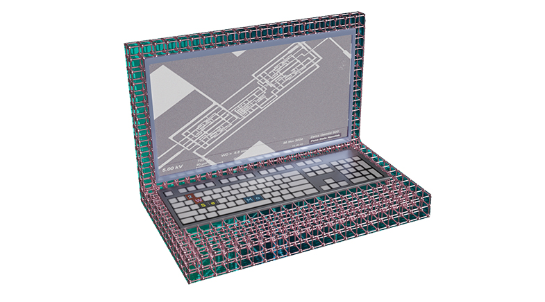
A theoretical computer architecture developed four years ago by two friends — Subir Ghosh and Mrinmoy Goswami — while working at a chip-making firm in Bengaluru has given the world its first non-silicon computer built entirely with two-dimensional (2D) materials.
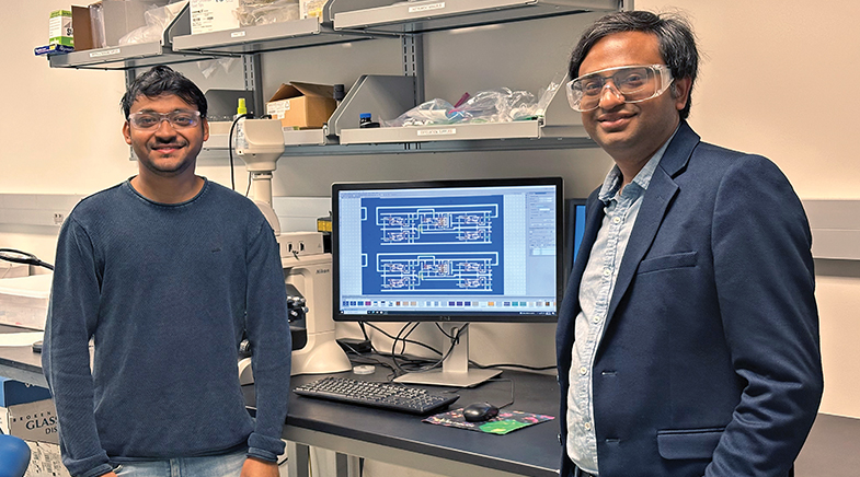
Ghosh and Goswami's One-Instruction Set Computer (OISC) architecture is at the heart of the atom-thick, non-silicon CMOS (complementary metal oxide semiconductor) technology-based computer recently built by a team led by Saptarshi Das, Professor of Engineering Science and Mechanics, The Pennsylvania State University, U.S. Ghosh, Das's graduate student, and Goswami, currently an engineer with technology company NVIDIA in the U.S., described their work in a paper recently published in Nature (bit.ly/CMOS-Ghosh).
For more than half a century, silicon has been the king of semiconductor technology. But scientists have been rethinking device architectures and exploring alternative materials to silicon, as there is little scope for further shrinking transistor sizes and accommodating more such devices in integrated chips. Two-dimensional materials have emerged as feasible alternatives, pushing the boundaries of semiconductor devices and functionalities.
These materials, with the thickness of an atom, came into focus with the discovery of graphene in 2004. A few years later, scientists commenced developing graphene-based transistors, making it a potential option for post-silicon electronics. Going a step further, in 2013, researchers at Stanford University's Robust Systems Group, led by Subhasish Mitra, Professor of Electrical Engineering and of Computer Science, built a working computer using transistors fashioned from carbon nanotubes (CNTs), yet another promising 2D material. Their contemporaries at the Massachusetts Institute of Technology further improved the technology by designing a microprocessor that consists of several thousand CNT transistors.
For the first time, a 2D material-based CMOS transistor technology, combining NMOS and PMOS transistors, has been built.
However, what the Penn State scientists have now achieved is a landmark feat. Scientists had earlier developed n-type metal oxide semiconductor (MOS) transistors and p-type MOS transistors from 2D materials. Now, for the first time, a 2D material-based CMOS transistor technology, combining NMOS and PMOS transistors, has been built. The CMOS technology, which currently relies solely on silicon, is at the centre of every electronic device in use today.
One of the key hurdles in efforts to move beyond silicon was the inability to develop an ideal CMOS technology using 2D materials, which would allow NMOS and PMOS transistors to work in tandem to achieve high performance at lower power consumption. Although past studies had successfully demonstrated small circuits based on 2D materials, they failed to scale up to complex, functional computers.
For the current study, the Penn State scientists fabricated NMOS and PMOS devices from large-area sheets of molybdenum disulphide and tungsten diselenide, grown through a metal-organic vapour deposition technique. The process, which involves vapourising ingredients, results in a chemical reaction, leading to the deposition of productions onto a substrate. The molybdenum disulphide layers have 1,000 NMOS, and the tungsten diselenide layers contain 1,000 PMOS. Through careful tuning of the device fabrication and post-processing, the scientists were able to adjust the threshold voltages of both n-type and p-type transistors, enabling the construction of fully functional CMOS logic gates. "There is an inherent advantage of using these layered 2D materials, which are atomically thin in nature," Ghosh says. Such nanosheets allow the stacking up of devices on top of each other, he says.
In comparison, even the latest commercially used silicon technology has a thickness of 6 nanometres (nm). When two silicon wafers are stacked on each other with a separation of 10 nm, the total thickness required is around 22 nm. "Now, think of using a 2D material which is 0.67 nm thin and the number of transistors that can be accommodated in that same height," Ghosh says.
The 2D materials, Ghosh says, are favourites not just of academia but also of industry. When silicon shrinks further, carrier mobility — how fast ions can go from one place to another — suffers. This is due to surface scattering, as well as quantum confinement. But the mobility numbers are high in 2D materials, says Ghosh, who worked with Goswami at DXCorr, before moving to Penn State for his PhD in 2022.
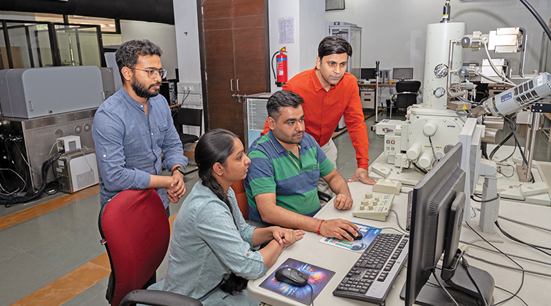
The work is pushing boundaries, says Kabeer Jasuja, Professor of Chemical Engineering at the Indian Institute of Technology (IIT) Gandhinagar. "Such a large-scale integration of 2D material-based CMOS circuits sets a solid foundation for a non-silicon platform," says Jasuja, who is not connected with the study. The Professor, who has been working on boron-rich 2D materials, points out that the work addresses "the most critical bottleneck" that the 2D materials-based CMOS technology currently faces: scalability. The findings, he adds, will also be relevant for research groups working in this field in India.
Offering a new class of dielectrics for 2D transistors could lead to smaller, faster, and more energy-efficient next-generation electronic devices.
"Our 2D CMOS computer operates at low-supply voltages with minimal power consumption and can perform simple logic operations at frequencies up to 25 kilohertz," says Ghosh. Even though the operating frequency is low compared to conventional silicon CMOS circuits, the 2D CMOS computer can still perform simple logic operations, he says.
Significantly, with the help of Shubham Sahay, Associate Professor of Electrical Engineering at IIT Kanpur and a co-author of the study in Nature, the team developed a computational model, which, upon calibration using experimental data and incorporation of variations between devices, could project the performance of the 2D CMOS computer and benchmark it against state-of-the-art silicon technology. "Although there remains scope for further optimisation, this work marks a significant milestone in harnessing 2D materials to advance the field of electronics," observes Ghosh.
Jasuja's work, interestingly, came to the attention of Penn State's Das when the latter was looking for materials with good dielectric properties. This led to a recent research collaboration between the two groups. Subsequently, Jasuja's PhD student Anshul Rasyotra spent six months in Das's lab at Pennsylvania. "The titanium diboride (TiB2) nanosheets that we discovered in our lab at Gandhinagar have excellent insulating properties and can thus become a high-performance insulator for 2D semiconductor devices," says Jasuja. The work was recently published in ACS Nano (bit.ly/TiB2-Jasuja).
Jasuja says that as transistors shrink to the atomic scale, finding suitable insulating materials becomes increasingly difficult. These nanosheets, created via a simple, room-temperature method, offer an equivalent oxide thickness of ~2 nm while maintaining excellent electrical properties — including low leakage current, ideal switching (60 mV/decade), and high on/off ratios — at just 1 V. 'This combination is rare and critical for low-power, high-efficiency electronics," he says.
What makes this work by Jasuja's team particularly promising is the scalability and stability of the material. The TiB2 nanosheets are thermally stable up to 125°C and withstand over a billion switching cycles, making them viable for real-world applications. By offering a new class of dielectrics for 2D transistors, this study could accelerate the development of next-generation electronic devices — smaller, faster, and more energy-efficient than ever before.
Subthreshold swing (SS) is a key performance metric in transistors, especially in low-power electronics. It describes how efficiently a transistor can switch from 'off' to 'on' as the gate voltage increases. When a transistor is off, a small leakage current still flows. As the gate voltage is slowly increased, the current increases exponentially until the transistor turns fully on. SS measures how much gate voltage is needed to increase the current by a factor of 10 (one order of magnitude) in this transition region. It's expressed in millivolts per decade (mV/decade). The lower the count, the better, because it means the transistor switches on faster and more sharply.
"The theoretical limit for SS at room temperature is 60 mV/decade for standard transistors. Achieving this means your transistor is switching as efficiently as physics allows — with minimal power loss and tight control over current," Jasuja explains.
Meanwhile, several Indian institutes are coming together to launch a major research programme into 2D materials-based electronics. The details of the project spearheaded by researchers at the Indian Institute of Science, Bengaluru, are still being worked out.


A higher orbit of connectivity
Tech advances, falling satellite-launch costs, and the demand for internet connectivity in remote regions are driving a satellite internet revolution.


Divide and conquer: The way to improve cancer treatment outcomes
Start-ups and indigenous research are finally stratifying cancer patients into groups, with the potential for improved outcomes.

Have a
story idea?
Tell us.
Do you have a recent research paper or an idea for a science/technology-themed article that you'd like to tell us about?
GET IN TOUCH