A new leaf
-
- from Shaastra :: vol 04 issue 01 :: Feb 2025

Sustainable substrates in electronics may be the answer to the mounting problem of e-waste.
The global electronics industry's 'take-make-waste' approach troubled Rakesh Rajendran Nair. The mounting problem of electronic waste (e-waste) — around 60 million tonnes of which are amassed every year — egged him on to look for a solution to e-waste while doing his doctorate under Professor of Optoelectronics Karl Leo and co-supervisor Hans Kleemann at the Dresden University of Technology (TUD) in Germany in 2022. Nair decided to work on developing eco-friendly substrates for printed circuit boards (PCBs) used in electronics.
PCBs are at the heart of electronic devices, including computers, mobile phones, household appliances and industrial control systems. Most PCBs typically use a substrate made of a composite material of woven fibreglass cloth and a flame-retardant epoxy resin. Silicon-based integrated chips are mounted on this substrate and connected with metal traces patterned on their surface. Such PCBs, discarded at the end of their life, are the most valuable components of e-waste, as they contain traces of precious metals such as silver, platinum, palladium and gold, apart from copper, nickel and others.
A typical PCB is nearly 30% metallic. Each tonne of PCB waste is estimated to contain roughly 130 kg of copper, 1.38 kg of silver, and 0.35 kg of gold. However, only a tiny fraction of PCBs that end up in landfills is recycled in an organised manner. Small recyclers tend to burn them in the open to recover valuable metals. The non-metallic part of the PCBs — the substrate — is not biodegradable or recyclable and is therefore dumped, harming the environment.
"There is a fundamental need for developing very sustainable substrates in electronics that meet different requirements," says Nair, currently a post-doc at TUD's Dresden Integrated Center for Applied Physics and Photonic Materials.
The TUD team found the leaf-derived material could be harnessed to create biodegradable electronic substrates.
Though efforts are being made to create PCBs with biodegradable polymers such as polylactic acid, such materials are expensive and require intricate processing. Scientists are trying other innovative materials to deal with PCB e-waste. A team in Austria, for instance, demonstrated in 2022 that fungal mycelium skin can be harnessed to make PCBs. Jiva Materials, a U.K.-based start-up, has developed a biodegradable and recyclable PCB substrate using natural fibres, a water-soluble polymer and a halogen-free flame retardant.
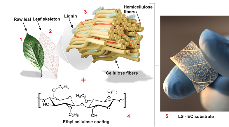
Nair's idea was to investigate the potential of using biopolymers abundantly found in nature: lignocellulose. The TUD team found that the leaf-derived material could be harnessed to create biodegradable electronic substrates. The work, published in the journal Science Advances in November (bit.ly/Leaftronics), led to the coinage of a new term, 'Leaftronics'.
"Scientists in the past, too, attempted to make devices on fresh leaves. But the problem with using a fresh leaf is that after a couple of days, the leaf will crumble and dry up, and thus the device will obviously not survive. This problem has not been solved to the best of our knowledge," Nair observes.
The TUD researchers returned to the leaf but used it in a different form. Their idea was to remove parts called the mesophyll, which made it unsuitable as a substrate. They wanted to check whether the quasi-fractal lignocellulose structure of the leaf, which serves as a scaffold for a leaf's living cells, could be a good substrate material.
"There is no way of creating such quasi-fractal structures that scale so many orders of magnitude — from hundreds of nanometres to a few centimetres — and repeat themselves. Even if one can, it will be very, very complicated," says Nair, who is a co-corresponding author of the paper with Leo.
They, however, found that when such leaf skeletons were coated with biodegradable polymer solutions, the materials absorbed these polymer molecules to form thin films. Such lignocellulose-reinforced polymer films could withstand temperatures as high as 260° Celsius (the temperature used for soldering electronic circuitry on the substrate) without any complex chemical stabilisation process. The scientists also demonstrated that the substrates could be used to make the latest thin-film devices, such as organic light-emitting diodes (OLEDs).
"We find that these substances are thermally, mechanically and chemically robust and thus can turn a new leaf in electronics," says Kleemann, who is a research group leader at TUD.
More important still was the fact that once the devices reached the end of their life cycle, the substrates could be easily decomposed in soil or through an enzymatic treatment, making it possible for the extraction of electronic components, apart from precious materials.
CIRCULAR PCB LIFECYCLES
Work is carrying on elsewhere, too. Reusability was the high point of a new type of PCB laminate developed by researchers at the University of Washington (UW) in Seattle. In April 2024, the team led by Vikram Iyer and Aniruddh Vashisth developed a new type of PCB laminate using a class of polymers called vitrimers. Iyer is an Assistant Professor at UW's Paul G. Allen School of Computer Science and Engineering, and Vashisth is an Assistant Professor at UW's Mechanical Engineering Department.
The work published in Nature Sustainability (bit.ly/vitrimers) said the material's performance was similar to those of conventional PCB substrates. Further, PCBs made from vitrimers could be turned into a jelly-like substance when treated with certain small molecule solvents, allowing for the extraction of components and reuse of the polymer material. The scientists claimed the vitrimer jelly could be repeatedly used to make new PCBs. They demonstrated that 98% of the vitrimer, 100% of the glass fibre and 91% of the solvent used for recycling could be recovered in each recycle.
This process allows for several paths to more sustainable, circular PCB lifecycles. Damaged circuit boards, such as those with cracks or warping, can be repaired in some cases. If irreparable, they can be separated from their electronic components, which can be recycled and reused. Similarly, the vitrimer and glass fibres can be recycled to make new circuit boards.
Ravinder Dahiya, Professor of Electrical and Computer Engineering at Northeastern University in the U.S., says he is aware of efforts to develop materials relevant to sustainable electronics but adds that the challenge would be to use them for mass manufacturing. "It will be quite challenging to upscale the work," Dahiya says.
GOLD EXTRACTION
Recovering valuable metals from discarded PCBs in an eco-friendly and energy-efficient manner is equally important. An international team of researchers led by Alireza Abbaspourrad, Associate Professor of Food Chemistry and Ingredient Technology at Cornell University, has developed a process to extract gold ions and nanoparticles from PCBs efficiently. Abbaspourrad's post-doctoral student Amin Zadehnazari has developed two vinyl-linked covalent organic frameworks (COFs) for adsorbing gold particles from e-waste. One of these COFs could capture 99.9% of the gold while minimising the uptake of other metals, such as copper and nickel, demonstrating a highly selective recovery process.
The methods currently employed to extract gold from e-waste involve using harsh chemicals, including cyanide, which harm the environment. On the other hand, the technique developed by Zadehnazari uses chemical adsorption and thus needs no hazardous chemicals. Also, the COF absorbs all gold particles in just an hour, unlike traditional methods that require 16-24 hours, says Zadehnazari.
In a paper published in Nature Communications (bit.ly/PCBgold) in December 2024, the team reported upscaling of the recovered gold into efficient catalysts for high-value reactions, such as converting carbon dioxide into carboxylic acid and other useful carbon-based chemicals. Zadehnazari says the gold is chemically pure and can even be used for more traditional uses with additional processing steps. He is confident that the technique will also help researchers design similar COFs for other valuable metals.
However, Dahiya believes that the sustainability of electronics is a broader issue than just dealing with e-waste. E-waste is an end-of-life issue, while the sustainability of electronics requires using materials designed for sustainability, which entails designing electronics to promote sustainability. He observes that this calls for the adoption of designs that allow reuse and repair.
In a 2022 paper (bit.ly/RavinderDahiya), Dahiya and colleagues argued the need for shifting the focus from e-waste management to a strategy of 'reduce, repair and reuse'. The recent emphasis on degradable electronics and the use of artificial intelligence to recover valuable materials from e-waste could also improve the circularity of the sector, Dahiya says.


Coming full circle
Transitioning to a circular economy is critical to addressing climate change, and the economic and other losses through wastage.

Twists in the quantum tale
TIFR physicists have produced a superconducting diode that works at high temperatures.


Stamp of honour
A glimpse of science milestones, as seen through the prism of philately.

Have a
story idea?
Tell us.
Do you have a recent research paper or an idea for a science/technology-themed article that you'd like to tell us about?
GET IN TOUCH