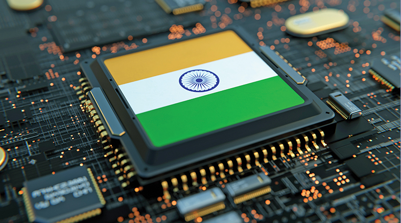
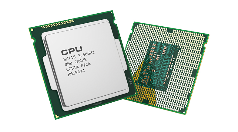
Semiconductor industry poised for a leap
-
- from Shaastra :: vol 04 issue 03 :: Apr 2025

Conditions are ripe for Indian semiconductor start-ups to bloom.
Scientists usually write proposals as the first step towards getting a grant for a project. At the Centre for Nano Science and Engineering (CeNSE), a multidisciplinary centre for nanoscale systems at the Indian Institute of Science (IISc), Bengaluru, researchers got ₹60 lakh just to write a proposal.
The year was 2015. The Indian government and the semiconductor industry had been in discussions on how to set up fabrication units in the country to manufacture chips. It was the second wave of discussions, after the first wave ended with a whimper about six years earlier. All the conversations at that time were about setting up silicon chip manufacturing units. The industry and bureaucrats recognised that it was tough and expensive, especially because no ecosystem existed on either side of chip manufacturing, either to develop materials that were used in the fab or to use the chips in devices after manufacture. Srinivasan Raghavan, a materials scientist who had joined IISc in 2006, looked around him and saw a developing ecosystem for a different semiconductor material: gallium nitride.
Gallium nitride was made towards the end of the 1980s by Japanese scientists as part of their work on light-emitting diodes (LEDs). Since then, it had been touted as a good candidate for semiconductor chips, with properties better than silicon for high frequency and high power applications. Japanese scientists Isamu Akasaki, Hiroshi Amano and Shuji Nakamura had won the 2014 Nobel Prize in Physics “for the invention of efficient blue light-emitting diodes” by growing gallium nitride. During his postdoctoral stint at The Pennsylvania State University in the U.S., Raghavan had learned how to grow gallium nitride in the lab. Around him, in CeNSE and other IISc departments, were people with the expertise to convert this material into devices, package them, and develop circuits. There were research groups in other institutions who could also chip in: at the Indian Institute of Technology (IIT) Bombay, IIT Madras, IIT Delhi, the Solid State Physics Laboratory in Delhi, and a few others.
Researchers at CeNSE reached out to the Ministry of Electronics and Information Technology (MeitY) and were asked to write a proposal. After spending ₹60 lakh over six months, they wrote a 2,000-page report suggesting an investment of ₹3,000 crore on a gallium nitride foundry. “An ecosystem for RF (radio frequency) and power electronics design exists in India,” says Raghavan. “So you can have a pull within India if you make the chip.” Gallium nitride chips were perfect for such applications. However, the ₹3,000 crore investment target seemed a high bar at that time. In 2021, after six years of discussions, the government approved ₹300 crore for a small fabrication unit.
This money was used to set up the Gallium Nitride Ecosystem Enabling Centre and Incubator (GEECI) at IISc, to develop gallium nitride technologies and incubate start-ups, which will have access to infrastructure and technical expertise at low cost. According to Grand View Research, an American market research and consulting firm, $2.56 billion worth of gallium nitride semiconductor devices were sold in 2023. The market is expected to grow at a compound annual growth rate of 26.4% from 2024 to 2030, with the main products being opto-semiconductors, power semiconductors, and RF devices. Compared to silicon, gallium nitride chips can work at higher power and temperature, making them suitable for two applications: in power electronics-based devices like mobile phones and electric vehicle chargers, and for transmitting wireless signals at high frequencies.
“(India) came to the scene late... The semiconductor sector worldwide has benefited from subsidies,” says MeitY Secretary S. Krishnan.
Raghavan and others had been training students on the technology as part of their PhD work. In 2019, one of them, Hareesh Chandrasekar, came back after a postdoctoral stint at the University of Bristol to lead a company, AGNIT Semiconductors, from CeNSE to make gallium nitride chips for defence products. A group of seven CeNSE researchers, including Chandrasekar and Raghavan, had founded the company as a way to commercialise gallium nitride products. The company raised $1.3 million in 2021 from former Cognizant CEO Lakshmi Narayanan and another $3.5 million in a seed round led by 3one4 Capital and Zephyr Peacock in 2024. Gallium nitride wafers are on United States’ International Traffic in Arms Regulations (ITAR) list, and so the U.S. government controls and regulates its export. “It’s a restricted and denied technology,” says Chandrasekar. “If you go to Raytheon today, they will probably sell you a radar with gallium nitride in it. But if you want to build your own radar and get gallium nitride semiconductors, you don’t get it.”
MONEY AT LAST
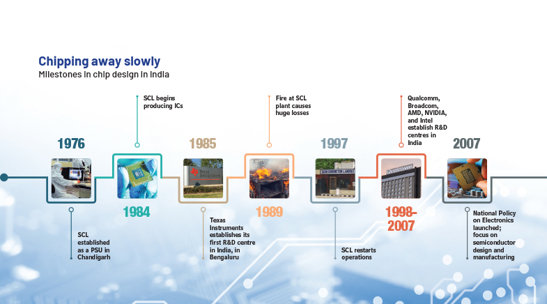
Semiconductor technology made its entrance in the country in 1976, with the establishment of the Semiconductor Complex Ltd (SCL, since renamed as the Semi-Conductor Laboratory) in Mohali. A fire broke out there in 1989, shutting the facility down for a decade after it had begun production. The fire set the country back in semiconductor technology by a decade or two. In a parallel development, Texas Instruments started an R&D centre in Bengaluru, the first of several such centres set up by multinationals. Over the next four decades, through the multinational development centres, Bengaluru became a global hub of chip design. India now is home to 20% of the world’s chip design engineers, the world’s second-largest pool, behind the U.S. However, the country had generated few homegrown product semiconductor companies. The economic value of all the design being done in India is, therefore, being captured elsewhere, in the headquarters of the multinational companies. “The real value will accrue to us if we own the IPR (intellectual property rights) of these chips and get the benefit of design plus manufacturing in India,” says Sanjay Nayak, former CEO of Tejas Networks, a telecommunication equipment company.
During the last decade, much of the discussions between the government and the industry revolved on reducing this loss of value in India. A set of domestic product companies, supported by domestic design and manufacture, would capture a significant part of the value in an electronics supply chain. Over time, a thriving domestic products industry would reduce the import bill, apart from providing support in strategic areas like defence. “We came to the scene late,” says S. Krishnan, Secretary, MeitY. “We didn’t understand that the semiconductor sector worldwide has benefited from subsidies.” When Intel came to India in the first decade of the century with the proposal of setting up a fab, India didn’t even have a scheme to provide subsidies for such ventures. As the discussions with the industry progressed over the decade, changes were provided to the policies to provide subsidies. A pivotal moment came during COVID, which disrupted supply chains around the world, forcing governments to realise the importance of self-reliance.
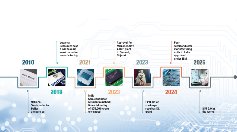
In 2022, the CHIPS and Science Act in the U.S. – to provide incentives to produce semiconductors – became law. It allocated $280 billion to research and manufacture of semiconductors and $52.7 billion in subsidies and tax breaks to domestic manufacturing companies in the sector. Similarly, the European Union passed the European Chips Act in 2023, which will mobilise more than €43 billion of public and private investments to foster innovation in the semiconductor space. In December 2021, the Indian government announced the India Semiconductor Mission (ISM), with a goal to establish India as a global hub for semiconductors. To be launched later in 2025, ISM 2.0 will look to take technologies in the research stage to market maturity.
In 2021, the government announced the India Semiconductor Mission, with a goal to establish India as a hub for semiconductors.
With a total outlay of ₹76,000 crore (about $9 billion), different schemes under ISM provide 50% financial support to semiconductor designers as well as manufacturers, aiming to create a foundation for semiconductor manufacturing. Since then, several State governments have announced their own addition to the funding, at an average of 25% of the cost. The policy was generous enough for aspiring semiconductor product start-ups to take the plunge. Overall, about 75% of the project cost is covered by subsidies, says Satya Gupta, President of the VLSI Society of India. He reckons that is a “strong incentive”.
In the past two years, several fabs, packaging units and assembly units have got approval and are being built. In 2024, the Tata group started fab work in a joint venture with Taiwan’s Powerchip Semiconductor Manufacturing Corporation (PSMC) in Dholera, Gujarat. The fab will focus on high-performance computer chips in the 28 nanometre (nm) node, which are used in applications like telecom receivers, Internet of Things (IoT), automobiles, radars, and several other products. In Sanand, 100 km from Dholera, Micron Technology is building an Assembly, Testing, Marking, and Packaging (ATMP) facility that is likely to go operational later in 2025. Kaynes Technology India is setting up an Outsourced Semiconductor Assembly and Test (OSAT) facility at Sanand. Close to 20 proposals are believed to be awaiting approval.
CHIPS IN AN ALPHABET SOUP
ASIC (Application-Specific Integrated Circuit): A custom-designed chip built for a specific application
ATMP (Assembly, Testing, Marking, and Packaging): Back-end semiconductor facility where chips are assembled and tested for functionality
FPGA (Field Programmable Gate Array): A semiconductor chip that can be reprogrammed after manufacturing for custom requirements
CMOS (Complementary Metal-Oxide-Semiconductor): A popular semiconductor fabrication technology
Moore’s Law: The observation that the number of transistors on a microchip doubles approximately every two years, leading to continued improvement in computing power and device performance
Node: The size of the smallest feature that can be created on a semiconductor chip during the manufacturing process

OSAT (Outsourced Semiconductor Assembly and Test): Back-end semiconductor facility for testing and packaging
SoC (System-on-a-Chip): A chip that integrates multiple functions (processor, memory, peripherals) onto a single chip
Although the global semiconductor value chain is highly distributed — design in one country, manufacturing in another, packaging in a third country, and so on — there are some critical players that exert an outsized control over the value chain. “Suppose the top five countries in the world in semiconductor industry sit down at a table to set some rules going forward,” says Nayak of Tejas Networks. “The question is: does India get a seat at that table?” The answer, currently, is ‘no’. India’s contribution to the global value chain of semiconductors has been negligible, with slow progress over the past few decades, despite the presence of a large number of engineers in the country.
The first acquisition in the sector was in 1999, when American telecom product company Broadcom bought Armedia, a Bengaluru-based chip design start-up, for $67 million. Despite this impressive start, only a few start-up companies were taken over in the next two decades: Cosmic Circuits by Cadence; Steradian Semiconductors by Renesas Electronics; Silicon and Beyond by Synopsys; and Saankhya Labs by Tejas Networks. “All of it put together is less than half a billion dollars in exits,” says Ganapathy Subramaniam, who founded Cosmic Circuits and is now a venture capitalist. “In Israel, to my mind, it is like $50 billion created. They may have one-tenth of our design talent in terms of numbers.”
This trend is finally beginning to change. The difference in the funding environment in the semiconductor space two decades back to now “is like night and day”, says Raja Manickam, Founder of Chennai-based iVP Semi and former CEO of Tata Electronics, the Tata group’s OSAT division. Government schemes like the Design-Linked Incentive (DLI) are also providing young design firms and start-ups with financial support to develop their products at scale. Encouraged by this shift, many founders have thrown their hat in the ring. Moreover, they are building products that can cater to India’s particular requirements.
FOR THE DEFENCE SECTOR
Mukul Sarkar started his solid state imaging lab in 2012, soon after he joined IIT Delhi as an Assistant Professor. By then he had spent a decade on the design of medical and imaging sensors, at multiple institutions in Europe. He set to work on developing an imaging sensor as soon as he started his lab in Delhi. Imaging sensors are at the heart of any camera system. They lie just beneath the optical lens and convert light into digital signals that are seen as an image.
Sarkar’s aim was to develop sensors with a high dynamic range, which is the capability to work in very low light to very bright light. The first set of PhD students that Sarkar got, around 2016, created a novel pixel design that helped them achieve very high dynamic range, especially towards the low-light regime. “Most cameras target higher light because lower light is difficult to detect,” says Sarkar. The lab’s low-light sensor was first designed for endoscopy, which has to work in conditions of low light.
COVID disrupted semiconductor supply chains around the world, forcing governments to realise the importance of self-reliance.
In 2019, Sarkar met Vrinda Kapoor and Vinayak Dalmia — both of whom had a business background. Dalmia and Kapoor had reached out to Sarkar looking for some efficient image processing algorithms. They teamed up to launch 3rdiTech (pronounced ‘Third eye tech’) in 2019 with the aim of commercialising image sensors. The first product was for defence: an imaging tool that works well in low-light conditions. “Much of what is currently used by the Indian defence forces is either high-cost, advanced technology or low-cost, low-efficiency products,” says Sarkar.
The alternative to low-light sensors are thermal imagers, which are required in pitch darkness, when there are no light particles at all. Low-light sensors can work on moonlit nights. Sensors from 3rdiTech work in moonlight. Later ones may work even during dark nights. The 3rdiTech team is now in the process of integrating its sensors into some defence equipment and starting field trials.
The image sensor is an Application Specific Integrated Circuit (ASIC) chip. Each of these chips has millions of transistors; they are manufactured in commercial fabs outside India. The prototype sensors are manufactured at the 180-nm node; the next version of the company sensors will be 65 nm. “I believe 65 nm is the end point at least for the next few years,” says Sarkar. The company is also working with the Indian Navy and the Indian Air Force. In September 2024, 3rdiTech entered into a technology partnership with the United States Space Force (USSF) to set up a multilateral semiconductor fab in India to manufacture specialised, security-focused chips.
Sensors form an important part of future defence technology, and defence is an attractive domain for Indian semiconductor start-ups. The sector is dependent on high technology, and most equipment use state-of-the-art semiconductors. This is why the U.S. and China, among others, are keen to see critical parts of the semiconductor industry operating within their borders. The Indian defence sector relies on imported technology, and can be an eager buyer of indigenously designed chips. In the context of the ongoing tariff wars and other restrictions, Sarkar flags a high risk: “If someday you’re not given access to – let's say – a fab in Taiwan, how will you fabricate those devices?”
Early semiconductor companies in India had come up partly because of defence work, and by being part of space missions. Now, as they improve in their capabilities, defence continues to provide opportunities for semiconductor start-ups. “In our experience, Indian commercial customers don’t entertain you unless you have a big brand name,” says Prasun Bhattacharyya, Chief Technology Officer at FermionIC Design, a Bengaluru start-up. “That problem is there in defence, too, but they entertain you because they face a shortage of chips.”
ENERGY EFFICIENCY
Aravind Prasad had been thinking about road safety ever since he lost a family member in a 2005 accident. As an engineer, he had recognised that modern technologies like Advanced Driver Assistance Systems (ADAS) could prevent many of these accidents. Despite the advantages, ADAS devices have not seen wide-scale integration in Indian cars, largely because of the cost. “The chipset in these devices is expensive,” says Prasad, who founded DeepGrid Semi in Hyderabad. “Even if I make the device today, it will cost me close to ₹10 lakh.”
DeepGrid Semi was started up in 2024 to address this problem. Prasad’s approach is to develop ADAS chipsets that can do real-time processing on the Edge, without having to send signals to a server far away. Such Edge chipsets also need to be scalable and consume low power. Once developed, these chipsets could be retrofitted in vehicles that have electronic steering and braking, which is about 30% of the cars on Indian roads. DeepGrid Semi is currently incubated at the Atal Incubation Centre-T-Hub in Hyderabad.
Computing on the Edge is a driver of future semiconductor technology, which is why it is attracting Indian semiconductor start-ups. At Thiruvananthapuram in Kerala, Netrasemi is developing AI/ML-based chips for Edge computing. “We’ve chosen computer vision as our domain because 40% of the Edge devices are vision-oriented,” says Netrasemi Chief Strategy Officer Hariprasad C. Computer vision is an area that generates high amounts of raw data. For example, every pixel in each frame of a 30 frames per second video is a data point, and so Edge devices need big compute capability. Chips for computer vision, therefore, are tuned for vector processing that can process an array of data at once.
Aravind Prasad of DeepGrid Semi is developing ADAS chipsets that can do real-time processing on the Edge.
The CPU requirement is high in such processors, and so the heat generated is high too. Netrasemi’s chips allow vector processing without the involvement of CPU. With their chip, the camera becomes AI-enabled and the processing happens on the device, instead of sending the raw content to the cloud or server and the processing happening there. Also, removing the CPU from the equation brings down the power requirement and heat generation. Such chips are useful for products in consumer electronics, industrial automation, and automobiles.
Energy efficiency, in general, is a driver of semiconductor development. At the Hyderabad incubator, Green PMU Semi is developing chipsets to harvest ambient energy and convert it into electricity. “Light, temperature difference, vibrations, and radio frequencies around us are typical sources of ambient energy,” says Sai Chandra Teja, Co-founder of Green PMU Semi. Energy harvesting is not a new concept, but recent material innovation has significantly improved the efficiency of transducers, which are responsible for converting physical energy into electricity. The greater the efficiency of a transducer, the larger the amount of ambient energy that will be converted to electrical energy. With better materials, the bottleneck of low-efficiency transducers has been addressed to a large extent, feels Teja.
A typical use case for Green PMU chipsets could be in smoke detectors fitted in buildings. These detectors depend on small coin batteries that need to be replaced periodically. Including an energy harvester chipset in the system would enable it to use ambient energy and extend battery life. The Green PMU Semi team has functionally validated its chips in the lab and will soon begin tests on customer boards.
COME A FULL CIRCLE
Arjun Menon’s first brush with a semiconductor fab happened as a five-year old. He was visiting his mother’s workplace, SCL, in Chandigarh. Nearly two decades later, in 2017, he visited SCL again. Menon was at that time working with Shakti, an open-source initiative by IIT Madras to develop an indigenous industrial-grade processor. It was one of Shakti’s earliest tape-outs.
Shakti was an academic project that was put together to help students develop a hardware-level understanding of a processor, and not just one based on simulations and models. Menon had joined project Shakti a short while after finishing his BTech at IIT Madras, where he got a chance to deepen his understanding of processors. That eventually paved the way for the next big step in his life: co-founding InCore Semiconductors in 2018.
InCore Semi makes RISC-V processors. RISC-V is an instruction set architecture (ISA), a set of standard instructions used in chip design, which is completely open source. It was released in 2016 to provide a free and open alternative to proprietary ISAs like ARM and x86. Many chip designers around the world, from large multinationals to young start-ups, have been gravitating towards it because it enables them to design cost-effective, low-power, and highly customisable processors.
Harnessing these properties, InCore has developed three types of processor cores – Azurite, Calcite and Dolomite – that can be used in a range of products from IoT and Edge AI to wearables and automobiles. “InCore’s processor cores are highly customisable and are designed in a way to enable users to automate their workflow,” says Menon.
Taken together, India’s chip design start-ups have started rewriting the script of the semiconductor industry. “We still have long, long way to go,” says Parag Naik, Co-founder of Saankhya Labs. But if this momentum continues, he reckons, “we should start to see some real change”.
'AN OPPORTUNITY FOR INDIA'
COURTESY: RENESAS

Renesas Electronics CEO Hidetoshi Shibata on how India can "leapfrog" over the West and China.
As CEO of Renesas Electronics, a Japanese semiconductor firm with deep interests in India, Hidetoshi Shibata has a ringside view of the semiconductor industry – as an observer and as a participant. Excerpts from an interview.
What are the big trends that will drive growth in the semiconductor sector?
The most obvious driver is the fast growth of artificial intelligence (AI). This will continue for a couple years, and we will see a lot more adoption of AI technology (in) Edge Computing. On top of that, innovations for greener economy, such as adoption of electric vehicles, reduced power consumption, battery technologies will drive the growth and consumption of semiconductors.
One key challenge, especially in Edge, is power consumption. Unlike with servers at the data centre, you don't have the luxury to be constantly plugged in with Edge devices. You need power-efficient architectures, materials and algorithms to enable broader adoption of AI on the Edge.
Does it need new approaches, or just better versions of what exists?
A bit of both. For the next few years, we can do with a better version of what we have. But ultimately, we need something totally different: a totally new material, for example.
The wide-bandgap material silicon carbide is one successful example of introducing new material in the semiconductor space. Something along that line will have to happen more broadly in the future.
How will these trends influence India and other countries trying to ramp up their presence in this space?
There is a tremendous opportunity for India, in two ways. One, the talent base of millions of competent engineers who speak English, and are well-versed in software... Tapping into this talent base makes the most logical sense.
If you look at the success of NVIDIA, yes, they have mastered the GPU hardware, but the key success ingredient for them was the software to use their hardware. India should be able to do something similar. Rather than just focus on hardware, you should pay equal attention to the software to use hardware and marry them in a seamless fashion. So people won't have a hard time marrying their software with semiconductor hardware devices that they procure from any supplier.
"If you apply... AI from the start in semiconductor design, you will leapfrog.. (over) the West, China."
The other angle is the possibility of doing semiconductor design from scratch using AI. You don't have any baggage. If you are successful in applying the fullest power of AI from the very beginning, chances are you will leapfrog... the West and China.
See also:


Structural reforms
The construction sector in India is in the throes of big change, embracing new materials and technology.

Nature's wonder material
From scaffolds that trap cancer cells to energy-efficient glazing, nanoscale cellulose finds new uses.

Have a
story idea?
Tell us.
Do you have a recent research paper or an idea for a science/technology-themed article that you'd like to tell us about?
GET IN TOUCH