

Ultra-thin,ultra-cool
-
- from Shaastra :: vol 05 issue 08 :: Aug 2026
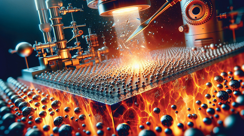
Scientists develop a scalable, low-temp method to develop quality tellurium films.
Tellurium as a semiconductor material in electronics has enormous potential: it offers faster transistors, more sensitive photodetectors and chemical sensors, and high-performance waste-heat harvesting devices. Manufacturing high-quality tellurium films has, however, been a challenge. But perhaps not for long.
Scientists from South Korea, India, and the U.S. have developed a scalable, low-temperature, semiconductor-compatible method to produce high-quality tellurium films, overcoming the manufacturing barrier. Such high-quality tellurium thin films, essential for electronics, have so far been developed with complex and expensive deposition techniques which operate at high temperatures and risk damaging heat-sensitive electronic substrates.
"Earlier studies showed that control deposition works only at high temperatures. Now, this work shows that you can deposit with better control even at low temperatures," says Satadeep Bhattacharjee, Head of R&D Division at the Bengaluru-based Indo-Korea Science and Technology Centre, and one of the authors of the study.
A scalable, low-temp, semiconductor-compatible method produces high-quality tellurium films.
For the study (bit.ly/films-thickness), the team used inert surfaces such as molybdenum disulphide or mica as the base for growing thin films. These slippery surfaces allow tellurium atoms to move freely and settle naturally. This base was kept inside an atomic layer deposition machine, and the temperature was set to 150° Celsius. Tellurium precursor gas was then put in the machine chamber. The gas atoms attached to the base surface, moved on the base as guided by the surface, and settled accordingly. When the surface was covered, the excess gas was flushed out, and another gas that converted tellurium precursors to tellurium atoms was introduced. This completed one cycle of deposition. More such cycles were repeated to form the film of desired thickness.
They then used a pre-trained machine-learning interatomic potential (MLIP) tool to understand the interaction between the tellurium atoms, between the base layer and tellurium atoms, and how they moved and grew on the base layer. They used a powerful quantum mechanical method, the Density Functional Theory (DFT), and studied the interaction between thousands of atoms. "Conventional DFT becomes computationally expensive. We therefore used a pre-trained MLIP tool." The atomic layer deposition technique is widely used in the semiconductor industry, and so manufacturers can easily follow it.










Shape of things to come
3D biomaterial platforms are revolutionising cancer research, paving the way for personalised therapy.

Tech gone wild
Researchers are aiding wildlife and forest conservation efforts with tech-enabled tools that examine a host of jungle sights and sounds.



Have a
story idea?
Tell us.
Do you have a recent research paper or an idea for a science/technology-themed article that you'd like to tell us about?
GET IN TOUCH