Defective is effective
-
- from Shaastra :: vol 05 issue 03 :: Mar 2026
Perfection may be overrated: scientists find that flaws in two-dimensional materials greatly enhance the material's properties.
Something in its purest form ought to be the best material for applications — or so the semiconductor industry believed in the 1950s, as it tried hard to make pure silicon for developing Integrated Circuits. When the industry finally made ultra-pure silicon, scientists realised it was practically useless for electronics applications, forcing them to create precise defects in the silicon by adding boron and phosphorus. Their work led to the development of p-type and n-type semiconductors and to a flourishing electronics industry.
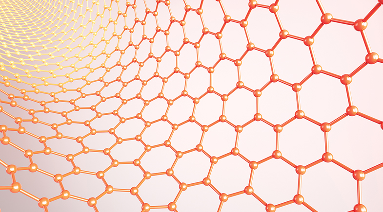
In the early 2000s, physicists at The University of Manchester engineered a new material called graphene. This nearly transparent single layer of carbon atoms in its purest form was 200 times stronger than steel, highly flexible, and a good conductor of heat and electricity. However, whenever graphene or any other two-dimensional material (with a single layer of atoms) with exceptional properties was manufactured, the lattice would show defects: missing atoms, an extra atom, a foreign atom, rough edges, and other distortions. These defects diminished the expected properties of the materials and took scientists back to the early 1950s. They began looking for methods to produce ultra-pure graphene and some other two-dimensional materials.
Missing, foreign or substituted atoms create special spots that can trap or conduct electrons differently than the material in its pure state.
Now, just as they did with silicon, scientists have started engineering defects in graphene. "Traditionally, because applications of graphene were in electronics, the defects were detrimental," says Ananth Govind Rajan, Associate Professor at the Bengaluru-based Indian Institute of Science. "But in the other areas, defects can be favourable, particularly in gas separation membranes, water purification membranes, filtration and light-emitting devices," Rajan, who works on two-dimensional materials, explains. Materials scientists have found that carefully engineered defects in two-dimensional materials can radically change a material's properties.
Sumeet Walia, Director of the Centre for Opto-Electronic Materials and Sensors at RMIT University in Melbourne, for instance, has developed an ammonia gas sensor using a single-layer molybdenum disulfide (MoS2). Surfaces of pristine MoS2 reacted quickly with gases, but the material had no selectivity towards ammonia. Walia's team heated MoS2 to 780° Celsius for a specific duration, giving some sulphur atoms enough energy to break free from the crystal lattice, leaving holes where they left the material. Molybdenum free of sulphur bonds interacted strongly with the nitrogen atoms of ammonia molecules, thereby increasing the sensitivity to the gas. The team also found that the sensor's performance improved when visible light was used. The defects and illumination together made the material more selective towards ammonia than other gases, such as carbon monoxide, hydrogen sulphide, sulphur dioxide, and nitrogen oxide. It also enabled rapid sensing, the team reported in a 2025 paper (bit.ly/ammonia-sensor).
WIDESPREAD APPLICATIONS
Defects can completely change a material's behaviour. Missing, foreign or substituted atoms create special spots that can trap or conduct electrons differently than the material in its pure state. "Every fundamental property gets tuned by the defects because of their (the defects') ability to interact with both light and electrical charges," says Walia. However, creating precise defects in single-layered materials is difficult, as the material may break during the introduction of the defect. The past two decades have provided scientists with tools such as sophisticated atomic-resolution microscopy, scanning tunnelling microscopy, aberration-corrected transmission electron microscopy, and atomic force microscopy to see and even manipulate individual defects in two-dimensional materials. Advanced chemical vapour deposition (CVD) systems allow scientists to precisely control the temperature, pressure, and gas flow, and to introduce defects during synthesis. Focused ion beams, low-energy irradiation, and laser and plasma processing also enable the creation of defects at exact locations without destroying the material. The resulting materials are being used in contemporary technology.
Using these tools, scientists have engineered defects which are being applied in catalysis, energy devices, ultrasensitive sensors, filtration membranes, quantum technologies and optoelectronic devices. For example, defects in these ultra-thin materials can trap energy and let it out in a single flash. Using this property, scientists from Rice University in the U.S. reported in 2025 the development of single-photon emitters that operated at room temperature by adding carbon to hexagonal boron nitride (bit.ly/Single-Photon). Such single-photon emitters produce light particles one at a time, allowing scientists to control and encode quantum information with precision, making it a useful resource for quantum computing and communication.
Artificial intelligence tools have now added a new dimension to defect engineering by leveraging imperfections to impart specific properties to materials.
When atoms go missing in two-dimensional materials, the sites where the atoms were present readily bind to other molecules. In 2022, scientists from the Switzerland-based École polytechnique fédérale de Lausanne (EPFL) used this property to demonstrate that when there were missing boron and nitrogen atoms in a single-layer hexagonal boron nitride, it was able to bind DNA effectively, and this property could be used for imaging DNA in biological samples (bit.ly/DNA-Imaging). This enhanced chemical reactivity can also be used for bioremediation. In 2020, Russian scientists showed that defect-rich graphene oxide with missing carbon atoms had holes that increased the material's capacity to capture radioactive forms of uranium 15 times and radioactive americium two times more than flawless graphene oxide (bit.ly/Absorption-Capacity).
Defects are places where the chemical reactions occur faster and more easily. In 2019, a team led by researchers from Eindhoven University of Technology in the Netherlands created sulphur defects in tungsten disulphide. The team showed that the defects in tungsten disulphide increased hydrogen production during the hydrogen evolution reactions in Proton Exchange Membrane water electrolysers (bit.ly/Sulphur-Defects).
In a collaborative research study published in 2021 (bit.ly/Missing-Atoms), British and Chinese researchers showed that MoS2 nanosheets with missing sulphur atoms increased the space to store more charge. The capacity to hold charge increased from 98 to 142 farads per gram. This was because the voids provided extra spots to hold charge. Researchers from the National University of Singapore have shown that defect-engineered graphene can be used for seawater desalination.
"If you can engineer the right shape and right size of these defects or nanopores, then you can control what goes through the pore, what doesn't go through (it)," explains Rajan.
DESIGNING THE PERFECT DEFECT
Artificial intelligence (AI) tools have now added a new dimension to defect engineering by leveraging imperfections to impart specific properties to materials. Scientists — such as IISc's Rajan — have been conducting simulations to predict the energy required to create a specific defect and assess its impact on material properties. Simulations are resource-intensive and time-consuming. To speed up the process, scientists are now developing Large Language Models (LLMs). "The idea is: given a lot of data from quantum mechanics, can we train surrogate ML (machine learning) models which will reduce the computational cost?" Rajan asks.
Rajan's group has developed a model that predicts how holes or nanopores created in a material by knocked-out atoms will affect its properties. The size and shape of the nanopores determine whether a molecule will or will not pass through the material, a property with applications in separation membranes, filtration, and even DNA sequencing. However, with millions of possible shapes and sizes, running simulations for each nanopore configuration is a challenge. To address this, Rajan's team first developed a way to describe holes in a text form, which was a step forward because the computer understands text-like data. They then created a dataset consisting of text names for several holes, along with their properties derived from simulations. This dataset was used to train an AI model, which now predicts the behaviour of new nanopores without running heavy simulations. The language model can be used to quickly search and design nanopore defects for filtration and other separation applications (bit.ly/LLM-defect-engineering).
NOVEL APPLICATIONS
Such tools in the field of defect engineering are helping scientists develop advanced materials for neuromorphic devices – brain-like devices that operate at high speeds while consuming low power. Defects in two-dimensional materials create controllable, memory-like electrical behaviour at the atomic scale, enabling them to function as artificial synapses (nerve junctions) with memory. Because two-dimensional materials are only one atom thick, even small defects can strongly affect how electricity flows through them, so little power is required to run these devices. "The entire memory mechanism is possible only through the defects," says materials scientist Viswanath Balakrishnan, Professor at the Indian Institute of Technology Mandi. Balakrishnan has developed a memristor: a tiny electronic device that remembers how much electricity has passed through it. A memristor changes its resistance when current flows through it, and it keeps that resistance change even after power is turned off. This property resembles that of brain nerve junctions, or synapses.
When Balakrishnan and his team began developing a memristor, they knew that pure tungsten diselenide (WSe2), though a semiconductor, was not the best material for a memristor. This was because there was no change in the material to seed memory when current flowed through it. Therefore, his team grew tungsten layers in a spiral shape with a twist between the layers. This twist, otherwise considered a structural defect and thus avoided, creates tiny irregular spots where current does not flow as usual, thereby allowing the material to act like a memory device. This material does not just switch "on" or "off" but also remembers the electricity that has passed through it. The team showed that a memristor made from this twisted material could work for 200 cycles and retain data for 15 minutes. A cyclic stability of 200 means that the memristor can be switched on and off without failing for 200 cycles; data retention of 15 minutes means that it can retain its stored state for 15 minutes after power is switched off. Both these values are low for developing a commercial application. Still, this proof-of-concept of the effect of structural defects opens avenues for further explorations of defect engineering in neuromorphic hardware (bit.ly/WSe2-memristor).
Engineering defects allow building systems that not only sense but also, for some time, store and process information.
As the use of large language models expands, their resource inefficiency becomes increasingly apparent, forcing scientists to develop advanced materials that mimic the brain. "We use defects as both memory and processing elements," says Walia, who has developed a neuromorphic vision sensor using MoS2 with tiny naturally occurring defects, which showed that the defects helped the material turn light into neuron-like electrical signals. The device fabricated using this material could detect changes in light and remember patterns, demonstrating that it has memory. Walia adds that engineering defects allow building systems that not only sense but also, for some time, store and process that information.
PRESERVING A DEFECT
Balakrishnan believes that without defects, a material becomes less "interesting". But the question is how many defects can be put on the material. "If you keep on increasing the defect density by knocking off the atoms one by one, at some point, the crystalline material may not remain stable," he says. Furthermore, preserving a defect is a challenge. "It (a material) becomes very prone to damage," he cautions. His team found that sulphur vacancies and other voids and cracks give single-layered tungsten disulphide excellent properties for applications in light-emitting diodes, electrolysis, and solar cells. However, this material degrades quickly, affecting its performance and restricting its applications in electronics.
The defects were letting in air and moisture, causing the damage. So, the researchers layered the defect-engineered material between transparent plastic-polydimethylsiloxane. They found that this plastic armour maintained the material's properties for longer. While bare tungsten disulphide degraded and lost 50% of its light-emitting quality over a year, the protected tungsten disulphide showed no degradation and fully retained its light-emitting quality. The plastic armour also helped the material stay intact even after it was bent 5,000 times (bit.ly/Plastic-Armour). "If you make a 2D material which is heavily defect-engineered, introduce a kind of encapsulation so that it can be stable for a long time," Balakrishnan suggests.
These are clearly exciting times for scientists working in the field. For many, the words of the British physicist, Sir Colin Humphreys, ring true. "Crystals are like people," he had said. "It is the defects in them which tend to make them interesting."


Chemical puppeteers
They're in your backyard, and they're deadly at creating 'zombies'. Their evolutionary adaptation holds exciting possibilities for biomedical research.

You've been blocked!
Digital detectives, aided by technology, are seeking to outpace cybercrime with powerful tools.

Susanne Mandrup on fat cells and human health
Biochemist and molecular biologist Susanne Mandrup on the importance of studying fat cells.

Have a
story idea?
Tell us.
Do you have a recent research paper or an idea for a science/technology-themed article that you'd like to tell us about?
GET IN TOUCH